Research
- Research Overview
- Organo Metallic Chemical Vapor Deposition
- Optical Response of Gold Nanoparticle Clusters
- Evanescent Wave Analytical Tools
- Surface Functionalisation
- Detection of Optically Active Molecules
- Optical Tweezers in Evanescent Fields
- Evanescent Microscopy and Spectroscopy
- Research Opportunities
- Research Group
- Former Coworkers and Students
- Collaborators
- Publications
Contact Information
Prof. Silvia Mittler
Physics & Astronomy 240
(519) 661-2111 x.88592
smittler@uwo.ca
FAX: (519) 661-2033

Research Overview
For more detailed on these topics, please follow the links or navigate using the menu at the left. I am currently interested in the following topics:
- integrated optical devices for sensor application
- metal nanoparticles of unusual shapes and clusters thereoff: nucleation, ripening, growth and their optical responses
- metal nanoparticles for sensor application
- optical tweezers in evanescent fields
- photonic crystals
- defined microporous materials in thin film geometry
- hollow optical fibers as smart cuvettes
- molecular nanoarchitectures of gold nanoparticles and organic functional material
- biocompatibility
- biomineralization
- alligned collagen
- evanescent microscopy for biological application
- molecular recognition reactions, guest-host systems, molecular imprinting, supramolecular science
- ultra thin polymer films
Organo Metallic Chemical Vapor Deposition (OMCVD)
In this current research project gold OMCVD precursors are used to grow covalenetly attached gold nanoparticles (AuNPs) on polymer surfaces. The main interest is to use these new metal structures for binding chemical and biological recognition sites via thiol (-SH) or sulfide bonds. On the other hand the nucleation and growth process of these new kind of nanoparticles is still not fully understood. Currently we are growing AuNPs on transparent polymers for sensor devices able to be fabricated in mass production.
Gold Nanoparticle Clusters and their Optical Response
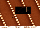
With the help of templates fabricated by laterally nano-structured self-assembled monolayers defined clusters of gold nanoparticles can be deposited by OMCVD. The optical response in two polarisation directions due to cross talk or other coupling mechanisms is studied.
Evanescent Wave Analytical Tools
Optical slab waveguides and fibres, as well as excited surface plasmons show evanescent fields reaching some hundrets of nanometers into the space above the device surface. These fields are used to detect chemical and biological reactions, typically guest-host or recognition reactions right on the surface of these devices.
Surface Functionalisation
In order to build a highly specific and highly sensitive sensor using the evanescent fields of an integrated optical device the surface functionalisation, responsible for the recognition reaction, has to be well engineered. Typically the functionalisations are formed by monolayers on top of the device offering its chemical or biological function right at the surface. Those monolayer films can be either fabricated via Langmuir-Blodgett-Kuhn technique or by self-assembling. In both cases the structure of the film, the functionality density and other parameters have to be optimised.
Detection of Optically Active Molecules with Means of Integrated Optical Devices
Optical active material can turn the polarisation direction of a light beam. The turning strength depends on the concentration, the interaction length between the light and the material as well as its optical activity, which shows a dispersion behaviour. In this project integrated optical devices, e.g. hollow optical fibers, will be used to measure the optical activity.
Optical Tweezers in Evanescent Fields
The evanescent fields of a channel waveguide acts as an optical tweezer to hold an object on top of itself. On the other hand a momentum is carried in the evanescent field in the direction of propagation. By using a channel waveguide objects are tapped on a channel surfaces and carried forward by laser pulses. The movement is correlated with adhesion forces between the object and the waveguide surface and can be tuned by chemical means (e.g. Coulomb interactions and pH control). Lateral patterning of the entire device surface should allow for defined stops and go's for light controlled microsfluidics.
Evanescent Microscopy and Spectroscopy
With this microscopy, WEFF and WEFS technology, and spectroscopy methodes in the evanescent field of a waveguide we can image objects at the very surface of a waveguide and are able to measure their absorption spectrum polarisation dependent. Typical examles are cell substrate interactions, the distances of cell adhesions, and the growth of bacteria biofilms.
last updated: October 2018


