


Research
- Silicon Photonics
- Space Weathering
- Defects in Semiconductors
- Positron Annihilation Spectroscopy
- Research Opportunities
- Publications
Contact Information
Prof. Peter Simpson
Physics & Astronomy 210
(519) 661-3390
psimpson [at] uwo [dot]ca
FAX: (519) 661-2033
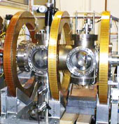
Positron Annihilation Spectroscopy
The Positron Beam Laboratory uses beams of positrons (the anti-particle of the electron) as a probe to study the structure of solids, especially electronic materials. Positron annihilation has unique sensitivity to vacancies, vacancy clusters and voids in materials.
The drive to develop nanometre-scaled materials and devices requires advanced characterization techniques that can function at these very small dimensions. Positron annihilation is one of very few techniques that can probe atom-sized defects in solids.
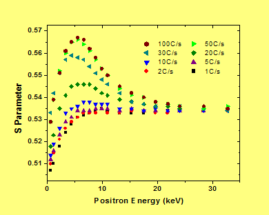
Positron annihilation data from silicon samples implanted with helium and then annealed to 800oC, varying the rate of ramping the temperature. The positron energy (x-axis) controls the probing depth into the sample, and the S-parameter (y-axis) measures open volume, in this case voids. We see that a rapid temperature ramp is required to form voids--- rapid heating permits the voids to form before the helium gas atoms are lost from the sample.
