
Recently there is considerable interest in finding a new class of materials which can be used to fabricate faster and smaller photonic and optoelectronic devices since semiconductor industry has reached its highest limit. In this research project we study photonic, plasmonics and optoelectronic properties of nanomaterials made form polaritonic/photonic band gap materials and doped with nanoparticles. These materials have energy gap in their energy spectrum. Energy gap in polaritonic/excitonic materials appears due to the phonon/exciton-photon coupling [fig 1a/1b]. In other words radiation signals in polaritonic materials are carried out by an admixture of photons and optical phonons/excitons rather than photons. On the other hand the energy gap in photonic materials is due the scattering of photons with periodicity of the dielectric constant (fig 1c). There is an analogy between polaritonic and photonic materials and semiconductors which have an energy gap in their electronic energy spectrum. When the energy of radiation signals lies within the band gap they are reflected. However, when the energy lies outside the band gap radiation signals propagate within these materials. Examples for photonic materials are photonic crystals and example for polaritonic materials are quantum dots and wires, III-V, II-VI semiconductors, polymers, dispersive materials; oxides, halides, organic and inorganic materials etc. Recently we have proposed fabrications of nanowires, nanowells, nanocavities, and nanofibers from these materials. To make electronic devices from semiconductors one has to dope n-and p-type (i.e. phosphorous, boron) impurities in semiconductors. Similarly, to make new types of photonic and optoelectronic devices from optical materials we have to dope them with an ensemble of nanoparticles such. Nanoparticles such as quantum dots, quantum wells [4a] and ZnO nanoparticles [4b] have been doped in these materials recently. To understand the optoelectronic properties of these materials we have applied probe and control lasers.This is a new research area which has been mainly started by my group. In this research area we are one of the leading research group in the world.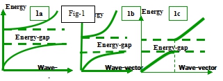
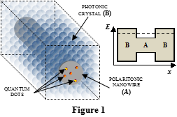
We have studied photonic heterostructures made by combining two or more photonic and/or polaritonic materials to form photonic waveguides, fibers and wires . These heterostructures use photonic band gaps to confine and direct the flow of light far more efficiently than traditional optical fibers/waveguides which rely on total internal reflection. An example of a photonic heterostructure is shown in Fig. 1, where polaritonic/photonic materials A and B are arranged so that A is embedded in B while the photonic band gap of A lies within that of B (side figure). In this case, photons with energy outside the band gap of A but inside the band gap of B are reflected by B and hence confined within A. Due to this band structure engineering, these systems also have quantized photonic states which can be modified by changing the size and shape of materials A and B. These types of structures have been recently experimentally realized .
 Analogous to the n- and p-type doping of semiconductors, the optical properties of polaritonic and photonic materials and photonic heterostructures can be controlled by doping them with nanoparticles (i.e. quantum dots). Nanoparticles have quantized electronic states which are controlled by the nanoparticle’s shape and size. A doped nanoparticle will interact with surrounding photonic band gap material via the electron-polariton or electron-photon interaction, depending on the material used. We have developed rigorous theoretical methods and numerical modeling techniques based on cavity quantum electrodynamics and the density matrix method to characterize and understand the optical properties of nanoparticle-doped polaritonic and photonic materials and heterostructures. By manipulating the light-matter interactions and dipole-dipole coupling along with band gap engineering we have discovered many phenomena such as the inhibition of spontaneous emission, photon-atom bound states, giant refractive indices, anomalous electromagnetically induced transparency, inhibition of one- and two-photon emission, anomalous Stark effects, dielectric catastrophes, and dark states.
© 1878 - Western University