


During the last 30 years significant success has been made in the development of theoretical and experimental techniques for investigation of solid surfaces and interfaces. Chemical composition, geometrical and electronic structure as well as the processes at the interfaces can now be investigated with unprecedented details. Fundamental knowledge from these studies has a big impact in the fields of semiconductor industry, photonics and catalysis.
Ongoing Research Projects:
Si and Ge quantum dots |
|
|
Electronic and optical properties of Si and Ge quantum dots Among quantum emitters semiconductor quantum dots (QD) have the highest emission rates and can be most easily integrated with semiconductor technology. QD emission properties often degrade because of various imperfections at the QD-dielectric interface. We investigate the electronic states and optical properties of Si and Ge quantum dots with variable size prepared by ion implantation in dielectic matrix by ion beam analysis, x-ray photoemission spectroscopy (XPS), photoluminescence (PL), and Raman spectroscopy. Learn more here... ...in collaboration with Peter Simpson |
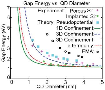 |
Quantum Confinement Models in Si and Ge Nanostructures We use perturbative effective mass theory as a toy theoretical model for quantum confinement(QC) in Si and Ge quantum wells (QWs), wires (Q-wires) and dots (QDs). Learn more here... ...in collaboration with David J. Lockwood, NRC |
|
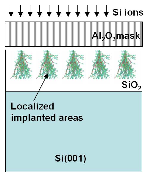
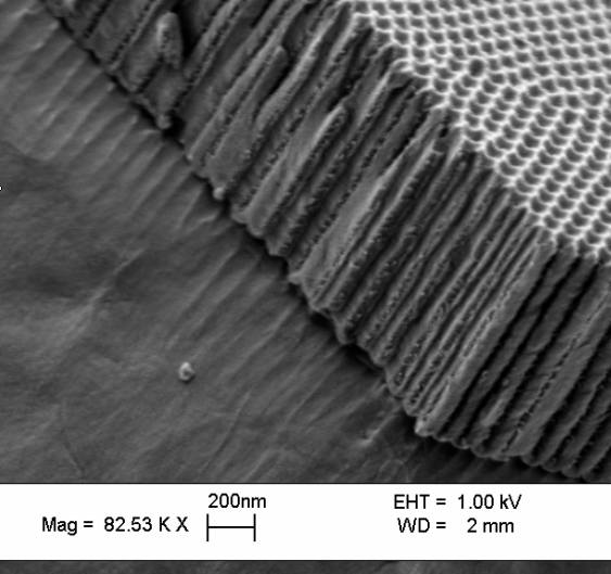
Nanoporous anodic Al2O3 films as ion implantation masks As a part of a larger project nanoporous Al2O3 films are developed as ion implantation masks to control lateral distribution and size of Si quantum dots. The ultrathin PAA films will be used in further experiments to explore its application to form silicon nanocrystal arrays as well as to characterize its damage profile upon bombardment with silicon and gold ions. |
  |
High-resolution ion beam analysis: transport and reactivity |
|
Exchange and interface growth in high-k dielectric stacks by medium energy ion scattering
|
 |
Diffusion of H/D in thin film materials using ERDA
|
|
Medium energy ion scattering (MEIS) and cold-neutron depth profiling (NDP) as a research tool for the study of surface oxides on metals
...in collaboration with Z. Tun (NRC, Chalk River), J.J. Noel (Chemistry, UWO) |
 |
Modification of low-dimensional materials properties using ion beams |
|
Modification of electrical and magnetic properteis of carbon-based materials Under construction... |
Collaborators:
David A. Crandles, Physics, Brock University
Eric Garfunkel, Chemistry & Chemical Biology, Rutgers University
Torgny Gustafsson, Physics and Astronomy, Rutgers University
Willy N. Lennard, Physics, UWO
David J. Lockwood, NRC, Ottawa
James J. Noel, Chemistry, UWO
Alexander Romanenko, Fermi National Accelerator Laboratory, Batavia, IL, USA
T.K. Sham, Chemistry, UWO
Peter J. Simpson, Physics, UWO
Zin Tun, Canadian Neutron Beam Centre, NCR, Chalk River
Funding
 |